A beautifully registered multi-layer board, with nice drilled holes, level copper plating, and no evidence of separation. This is what we strive for in the manufacturing of printed circuit boards.
But, let’s face it, there are things that can go wrong. Lots of things that can go wrong. It’s up to you as engineers and senior managers to ensure that people are trained to understand where all these problems and issues can come from and how to address them.
What could possibly go wrong? Well, a lot!
Delamination
Delamination is the most critical issue. This is where you have separation of either the resin from the copper foil, from the indium for the internal layers, or blisters within the laminate resin itself. The issue is that when you have delamination, you usually only see it after the production process when the board is ready to ship. How do you know if the issues arose during lamination process, or the oxide or oxide alternative process? It could because of the pressure of drilling, it could be a routing, it could be assembly steps. If you have delamination, you’ll be troubleshooting all the way down the supply chain.

Line Width Issue
Here’s what you’re looking for: the resist with the conform wall, sitting nicely on the copper foil surface, it has been exposed and then developed away, and now you're going through the etch to dissolve away the unwanted copper. However, what can happen is if you don't have good confirmation of that resist to the copper surface through the pore cleaning, issues with lamination of the resist to the copper, it can expose the sidewall of the photoresist that's protecting the copper and it exposes that in such a way that more copper it's dissolved away.

Issues with surface prep
On the left, you can see the photoresist has been exposed on the inner layer, it's been developed away. In the copper field, it looks like a hole or a defect because there were issues with it not conforming to the copper surface. It could be a particle matter, it could be a dent in the copper foil, it could be some damage in the copper foil. Regardless, it's there and when you go into etch, you can see on the right-hand side some of that copper has been etched away and that's going to be rejected because that's more than 10 percent of the copper thickness. That's an issue and you'll end up losing that job.

DES Process Defects
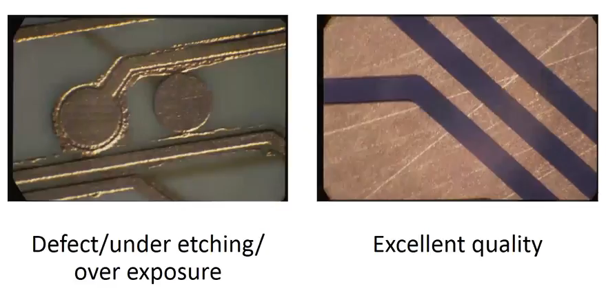
Here’s another issue that will have you traveling down the troubleshooting rabbit hole. What caused these? Imaging? Under etching? Overexposure? Something else? You have what looks like that nicely exposed resist over the copper surface prior to etch, but you don't know if there are any working issues of poor adhesion, that can lead us into significant defects. You don't know that until you actually etch that layer and then you're going to find out: Do I have mouse bites? Have I lost some of my circuit trace? Maybe I've lost it off, maybe it's an open. All of those things are very critical.


